


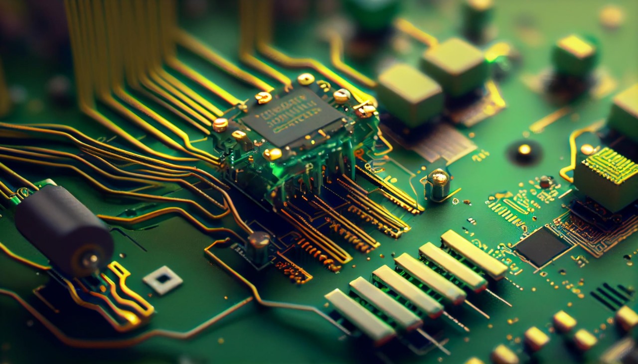
A printed circuit board (PCB) is an essential component in modern electronics. Its main role is to provide both mechanical support and electrical connections for the various components mounted on it. This is achieved through a network of copper wires, which act as pathways, enabling electrical signals and power to flow between the components.In simpler terms, think of a PCB as the backbone that holds everything together in your electronic device. It acts as a platform for connecting and supporting components such as integrated circuits, resistors, capacitors, and connectors.
Brief Introduction What Is PCB
Now that we know the basic function of a PCB, let’s dive into the crucial aspect of PCB layout design. Once the schematic design of a project is completed, the next step is to carry out the PCB layout design. This process is extremely important, as it directly affects the overall functionality of the design.In order to successfully debug the circuit design of a chip, it is crucial to have a well-planned and efficient PCB layout. With that in mind, we will discuss nine key points that you should consider when designing a PCB layout.By following these recommendations, you can optimize your PCB layout design and maximize the performance and reliability of your electronic device. So, let’s get started with some valuable insights on PCB layout design!
Nine Ways To Better Optimize PCB Layout Design
In the realm of integrated circuit application design, one important step that follows the completion of the project schematic design is the PCB layout design. This process holds immense significance as it directly impacts the overall functionality of the design.
Consequently, it is imperative to ensure a practical and efficient PCB layout for successful chip circuit design debugging. In this article, we will discuss the key aspects that should be considered during PCB layout design.
1. Component package selection
Resistance selection: The selected resistance can withstand voltage, maximum power consumption and temperature can not exceed the use range.
Capacitor selection: The selection also needs to consider the voltage resistance and maximum effective current of the selected capacitor.
Inductor selection: The effective current and peak current of the selected inductor must be greater than the current flowing in the actual circuit.
2. Common interference in circuit design
Crosstalk: When the parallel running distance of the design line is too long, the mutual capacitance and mutual inductance between the wires will couple the energy to the adjacent transmission line. Crosstalk effects can be reduced by:
Add safety cabling

Make adjacent lines perpendicular to each other as much as possible

Each distance of parallel lines increases the distance between the two

Reflection: The impedance mismatch on the transmission line due to too many corners and branches of the wiring can be improved by reducing corners and branch lines on the line or avoiding right Angle routing and branch line reinforcement.

3. Determined Drounding Mode
Single-point grounding (for low-frequency circuits) : All circuit grounding wires are connected to the same point of the common ground wire, which is simple to connect and reduces interference between ground wires and loops.

Multipoint grounding (for multilayer circuit/high frequency circuit) : Each part of the system is grounded nearby to provide a low grounding impedance.
4. Add Filter And Bypass Capacitance
To ensure a stable input/output voltage, increase the input/output capacitance.

Add a bypass capacitor between the power supply and the IC to ensure input voltage stability and filter out high-frequency noise.

5. Impedance position design
Relatively speaking, the higher the impedance, the easier it is to be interfered with. The PCB impedance position of a synchronous buck chip is designed as follows.

6. Power/ground handling
Even if the wiring in the entire PCB board is completed well, the interference caused by the inconsiderate power supply and ground wire will reduce the performance of the product. When wiring, try to widen the width of the power supply and ground wire, it is best that the ground wire is wider than the power line, and their relationship is: ground > power line > signal line.
The PCB of the digital circuit can be composed of a wide ground wire to form a loop, that is, to form a ground network to use (analog circuits cannot use this method).
A large area of copper layer is used as ground wire, and the places that are not used on the printed board are connected with the ground as ground wire. Or make a multi-layer board, the power supply, the ground line occupy a layer.
7. Common ground processing of digital and analog circuits
Common ground processing of digital circuit and analog circuit: When digital circuit and analog circuit coexist, the wiring needs to consider the mutual interference problem, especially the noise interference on the ground wire.
The frequency of the digital circuit is high, and the sensitivity of the analog circuit is strong. For the signal line, the high-frequency signal line is as far away from the sensitive analog circuit device as possible.
For the ground wire, the entire PCB external connection boundary has only one port, so it is necessary to deal with the problem of digital and mode common ground inside the PCB, and the digital and analog inside the board are actually separate from each other, only at the port of the PCB and the outside world (such as plugs, etc.), the digital and analog are a little short, please note, There’s only one connection point.
8. Signal line Distribution layer
Signal line distribution on the power (ground) layer: in the multi-layer printed board wiring, because there is not much line left in the signal line layer, more layers will cause waste and increase a certain amount of work for production, and the cost will also increase accordingly.
To solve this contradiction, wiring on the electrical (ground) layer can be considered. The power layer should be considered first, followed by the formation. Because it is better to preserve the integrity of the formation.
9. Signal Direction Design
When designing the PCB layout, the design principle of placing in a straight line along the signal flow direction should be fully observed, and it should be avoided as far as possible.


Write For Us Technology is a trusted platform for sharing expert-driven insights on modern technology, digital marketing, and emerging innovations. Our editorial team includes SEO professionals, developers, and tech writers who actively work in the industry and bring practical, real-world experience to every article.